
Danish nanowires have great potential
Danish nanophysicists have developed a new method for manufacturing the cornerstone of nanotechnology research – nanowires. The discovery has great potential for the development of nanoelectronics and highly efficient solar cells.
It is PhD student Peter Krogstrup, Nano-Science Center, the Niels Bohr Institute at the University of Copenhagen, who developed the method during his dissertation.
- We have changed the recipe for producing nanowires. This means that we can produce nanowires that contain two different semiconductors, namely gallium indium arsenide and indium arsenide. It is a big breakthrough, because for first time on a nanoscale, we can combine the good characteristics of the two materials, thus gaining new possibilities for the electronics of the future, explains Peter Krogstrup.
We can capture more of the sun’s light
Today only approximately 1 % of the world’s electricity comes from solar energy. This is because it is difficult to convert solar energy into electricity. It is a great advantage for the researchers to be able to combine different semiconductors in the same nanowire.
- Different materials capture energy from the sun in different and quite specific absorption areas. When we manufacture nanowires of gallium indium arsenide and indium arsenide, which each have their own absorption area, they can collectively capture energy from a much wider area.
We can therefore utilize more solar energy, if we produce nanowires from the two superconductors and use them for solar cells, explains Peter Krogstrup.
The nanowires of gallium indium arsenide and indium arsenide also have great potential in nanoelectronics. They can, for example, be used in the new OLED displays and LEDs. But it requires sharp transitions between the two materials in the nanowire.
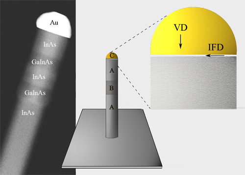
A nanowire made of the two semiconductors gallium indium arsenide (GaInAs) and indium arsenide (InAs) with gold (Au) as a catalyst. To the right a schematic illustration of the new cultivation method, where the semiconductor materials can move both from the top of the gold droplet and from the underside.
No soft transitions
The cultivation of nanowires takes place in a vacuum chamber. The researchers lay a gold droplet on a thin disc comprising of the semiconductor and the nanowire grows up from below. In the transition between the two semiconductor materials in the gold droplet there was previously a mixing between the materials in the gold droplet and there was a soft transition between the materials. With the new method both of the materials can go from the top of the gold droplet or from the underside of the gold droplet. When the material comes from the underside, there is no mixing of the semiconductor materials. There is therefore a sharp transition on the atomic level between the gallium indium arsenide and indium arsenide.
- This sharp transition between the two semiconductors is necessary for the current – in the form of electrons, to be able to travel with high efficiency between the two materials. If the transition is soft, the electrons can easily get caught in the border area. The new mixed nanowire can be beneficial for many areas of nano research around the world, says Peter Krogstrup, who has been working at the Danish III-V Nanolab, operated in collaboration between the University of Copenhagen and the Technical University of Denmark.
A new collaboration between the company SunFlake A/S and The Danish National Advanced Technology Foundation has been kicked off this week. SunFlake A/S uses nanowires to develop prototypes of solar cells and they can also benefit from the new method in their continuing work. The nanophysicists’ discovery has just been published in the prestigious scientific journal Nano Letters.
Contact
PhD student Peter Krogstrup, Nano-Science Center (www.nano.ku.dk), Niels Bohr Instituttet (www.nbi.ku.dk), Københavns Universiet på mail: krogstrup@fys.ku.dk or mobile: +45 26 71 51 91
Communication Officer Gitte Frandsen, Nano-Science Center (www.nano.ku.dk), Københavns Universitet på mail: gf@nano.ku.dk or mobile: +45 28 75 04 58
Link to paper in Nano Letters: Junctions in Axial III−V Heterostructure Nanowires Obtained via an Interchange of Group III Elements, Nano Letters https://pubs.acs.org/doi/full/10.1021/nl901348d